TSMC reveals detailed specifications of 1.4nm! Power consumption drops by 30%, showing wafer-level c
The 2nm battle is imminent, and chip manufacturing is rushing towards the angstrom era.
According to a report on April 24, TSMC released its next-generation cutting-edge logic process technology A14 (1.4nm) at the North American Technology Seminar today. A14 is scheduled to be put into production in 2028, and the development is progressing smoothly. The yield performance is better than expected. The upgraded version of A14 that supports back-side power supply will be launched in 2029.
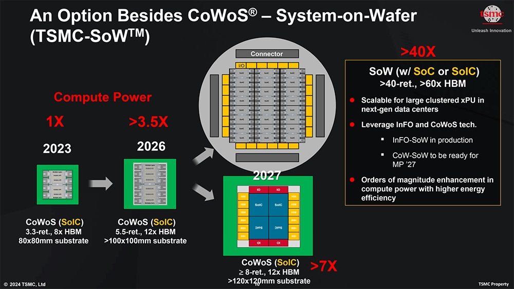
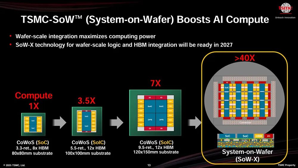
At the same time, TSMC launched new logic processes, special processes, advanced packaging and 3D chip stacking technologies for the first time. Among them, SoW-X technology can build a wafer-level system that can integrate at least 16 large computing chips, memory chips, fast optical interconnects and new technologies on a substrate as large as a dinner plate, providing chips with several kilowatts of power, and computing power is expected to reach 40 times that of existing CoWoS solutions.
In contrast, Nvidia's current flagship GPU is composed of two chips spliced together, and the Rubin Ultra GPU expected to be launched in 2027 is composed of four chips spliced together.
TSMC announced that it will build two new factories near its wafer fab in Arizona, USA. In the future, it will plan 6 wafer fabs, 2 packaging plants and 1 R&D center to expand production in the United States.
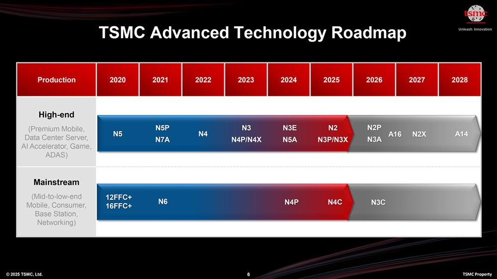
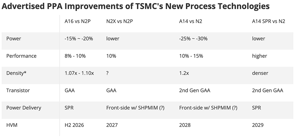
In addition, the company revealed that it will start producing chips based on the performance-enhanced N3P (third-generation 3nm-level) process technology in the fourth quarter of 2024. The N3X chip is expected to be mass-produced in the second half of this year. Compared with N3P, N3X is expected to increase maximum performance by 5% at the same power, or reduce power consumption by 7% at the same frequency, and support voltages up to 1.2V.
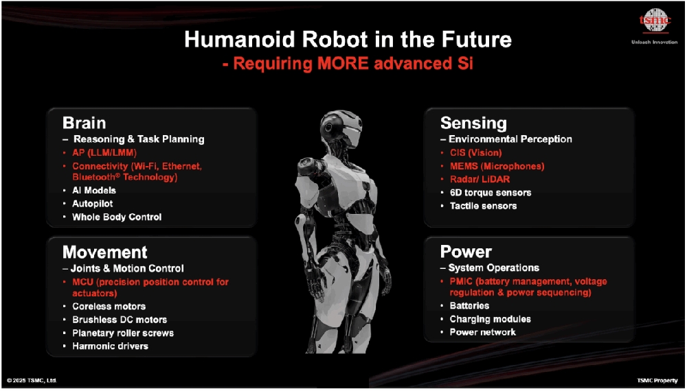
TSMC also posted a picture of a humanoid robot, marking the various advanced chips required. The ability to integrate these chips into high-density, energy-efficient packages is critical.
01. A14 process is close to mass production: power consumption is reduced by 30%, and NanoFlex Pro is enabled
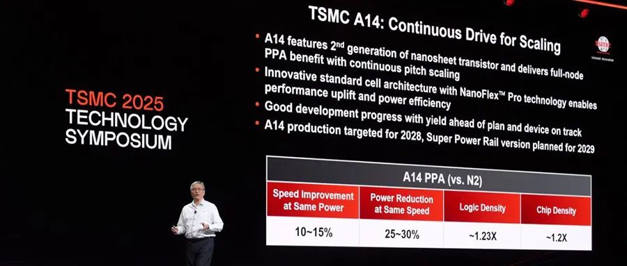
TSMC revealed that the new A14 process will use the second-generation GAAFET nanosheet transistor, and will provide higher performance, energy efficiency and design flexibility by upgrading its NanoFlex standard cell architecture to NanoFlex Pro technology.
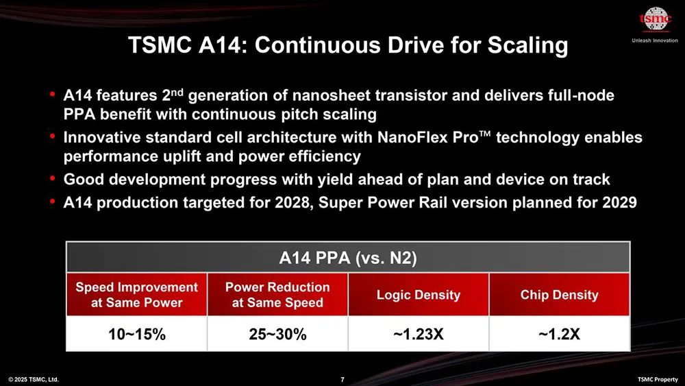
Compared to the 2nm-class N2 process that will be mass-produced later this year, the A14 will be 15% faster at the same power consumption, or 30% lower power consumption at the same speed, while the logic density will be increased by more than 20%.
NanoFlex Pro is a design technology co-optimization (DTCO) technology that allows designers to design products in a very flexible way by fine-tuning the transistor configuration to achieve the best power, performance, and area (PPA) for specific applications or workloads. This technology will go into production in 2028, and the first version will not have back power supply.
TSMC plans to launch the A14 with support for super power rail (SPR) back power supply in 2029. The company has not yet revealed the specific name of the process technology, but according to TSMC's traditional naming method, it can be speculated that it may be called A14P. The A14 is expected to launch its highest performance version (A14X) and cost-optimized version (A14C) after 2029.
Since A14 is a brand new node, it will require new IP, optimization, and EDA software compared to N2P (leveraging N2 IP) and A16 (N2P with backside power supply).
▲TSMC's announced chip density reflects a "hybrid" chip density, including 50% logic, 30% SRAM, and 20% analog. **Same area, same speed. (Source: Tom's Hardware)
TSMC 16A is the first version of SPR, with backside power supply. SPR is designed to improve signal routing and power transmission for AI/HPC designs. A16 is expected to go into production in the second half of 2026. Compared with N2P, A16 is 8-10% faster at the same power and 15-20% lower power at the same speed.
Unlike A16, N2, and N2P, A14 does not have an SPR backside power supply network (BSPDN), which can target applications that cannot get practical benefits from BSPDN, but this requires additional costs.
Many client, edge, and professional applications can take advantage of the additional performance, lower power consumption, and transistor density brought by TSMC's second-generation GAA nanosheet transistors. These applications do not require dense power routing, and traditional front-side power supply networks can meet the needs.
TSMC plans to put chips based on A14 process technology into production in 2028. Considering that A16 and N2P will start mass production in the second half of 2026 (i.e., the end of 2026), and the chips will be available in 2026, Tom's Hardware speculates that the target production time of A14 is the first half of 2028, which is expected to meet the needs of customer applications launched in the second half of the year.
02. A large wave of new process and packaging technologies are launched for the first time, specializing in HPC, mobile phones, automobiles, and the Internet of Things
In addition to A14, TSMC has launched new logic processes, special processes, advanced packaging, and 3D chip stacking technologies for the first time, contributing to a wide range of technology platforms such as high-performance computing (HPC), smartphones, automobiles, and the Internet of Things (IoT). These products are designed to provide customers with a full set of interconnect technologies to drive their product innovation, including:
1. High-performance computing
TSMC continues to advance its CoWoS technology to meet AI's continued demand for more logic and high-bandwidth memory (HBM). The company plans to achieve mass production of 9.5-inch reticle-sized CoWoS in 2027, integrating 12 or more HBM stacks with TSMC's leading logic technology in a single package.
Following the demonstration of its system-on-wafer (TSMC-SoW) technology in 2024, TSMC has launched a CoWoS-based product SoW-X, which aims to create a wafer-sized system with 40 times the computing power of existing CoWoS solutions. Mass production is scheduled for 2027.
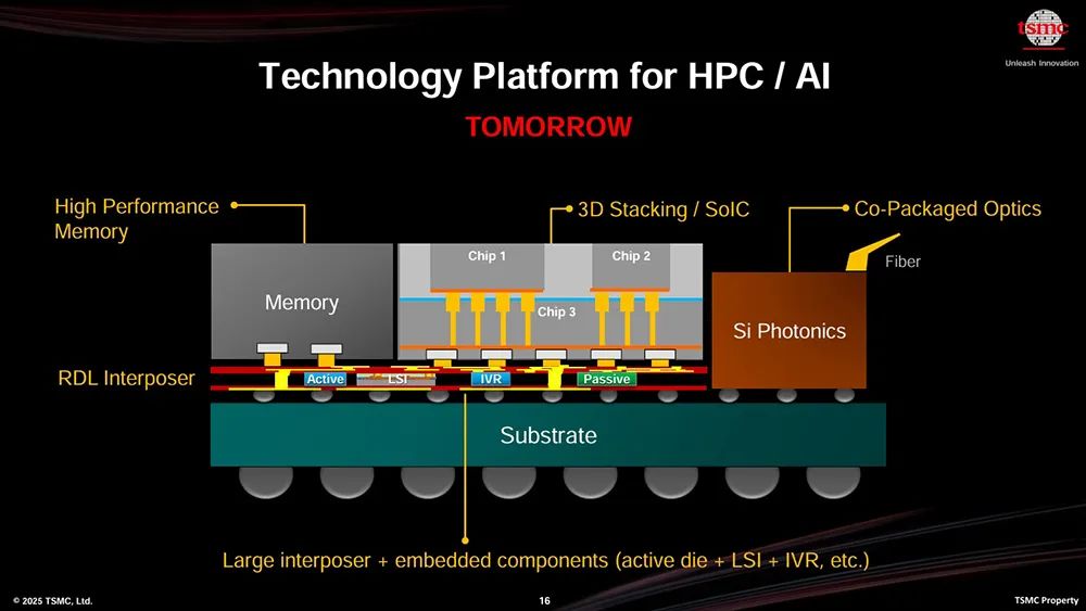
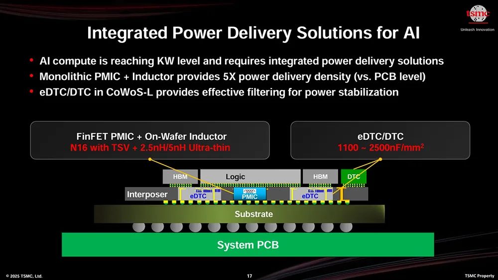
TSMC offers a range of solutions to enhance the computing power and efficiency of its logic technology. These solutions include silicon photonic integration with TSMC's Compact Universal Photonic Engine (COUPE), N12 and N3 logic substrates for HBM4, and a new integrated voltage regulator (IVR) for AI, which has a 5x increase in vertical power density compared to separate power management chips on the board.
2. Mobile phones
TSMC is using its next-generation RF technology, N4C RF, to support AI on edge devices and their need for high-speed, low-latency wireless connections to transmit massive amounts of data. Compared with N6RF+, N4C RF has a 30% reduction in power consumption and area, which is ideal for packaging more digital content into RF system-on-chip (RF) designs to meet the requirements of emerging standards such as WiFi-8 and AI-rich true wireless stereo. The technology is scheduled to be put into risk production in the first quarter of 2026.
3. Automotive
Advanced driver assistance systems (ADAS) and autonomous vehicles (AV) have stringent requirements for computing power without sacrificing automotive-grade quality and reliability. TSMC is meeting customer needs with its advanced N3A process, which has passed the final stage of AEC-Q100 Level 1 certification and continues to improve defects to meet automotive parts per million (DPPM) requirements. The N3A process has begun to be applied to automobile production, injecting a full set of technologies into future software-defined cars.
4. Internet of Things
As everyday electronic products and home appliances adopt AI functions, IoT applications are taking on heavier computing tasks, while battery life remains stretched. TSMC's previously announced ultra-low power N6e process is now in production and is targeting the N4e process to continue to break through the energy efficiency limits of future edge AI.
03. Conclusion: TSMC steps up research and development and rushes into the Angstrom era
The A14 represents a major advancement in TSMC's industry-leading N2 process, designed to drive AI transformation by providing faster computing speeds and higher energy efficiency. It is also expected to enhance the built-in AI capabilities of smartphones.
Dr. Wei Zhejia, Chairman and CEO of TSMC, said that TSMC's technological leadership and excellent manufacturing capabilities provide customers with a reliable innovation roadmap. TSMC's cutting-edge logic technology is part of a comprehensive solution that connects the physical and digital worlds, aiming to unleash customers' innovative potential and promote the future development of AI.
Zhang Xiaoqiang, senior vice president of business development at TSMC, revealed that with the rapid development of AI, companies that design large AI chips have become the fastest customers to introduce new process technologies, driving the continued growth of advanced processes. He expects the annual output value of the global semiconductor industry to exceed $1 trillion by 2030, but investors still need to observe carefully in the face of concerns such as the recent increase in tariffs by the United States and the AI bubble.
Benefiting from the rising demand for computing power in the development of AI, as well as its technical and mass production advantages in advanced processes and advanced packaging, TSMC is leading the 2nm process competition, and Apple and AMD are likely to be the first customers. Not long ago, AMD also confirmed that its Zen 6 Venice server chip will be manufactured using the N2 process node. According to Taiwanese media reports, Intel has ordered N2 from TSMC. Nvidia and MediaTek are also expected to be major customers of TSMC's advanced process. In addition to the much-anticipated 2nm process, most computer, tablet and mobile phone chips that will be launched in the next few quarters will be manufactured using TSMC's 3nm process technology.