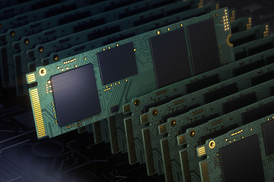
TSMC prepares to produce HBM4 basic chips: use N12ffc+and N5 process technology
In response to the current demand of the artificial intelligence (AI) market, it is expected that the new generation of HBM4 storage will have several main changes with the current HBM products. The most important of which is the memory stack link interface standard, which will be already a 1024 -bit that is already very wide. Further turn to the ultra -wide 2048 bits, which makes the HBM4 memory stack link links will no longer be the same as usual. Chip suppliers will need to use more advanced packaging methods than they are now to accommodate the ultra -wide memory of the stack link interface.At the 2024 European Technology Symposium held a few days ago, TSMC provided some new details about basic chips for HBM4 manufacturing next. In the future, HBM4 will use logic process to produce. As TSMC plans to adopt the improved version of its N12 and N5 process to complete this task. Compared with the current basic chip of storage suppliers, such advanced chips, this development is expected to make TSMC occupy a favorable position in HBM4 manufacturing.
According to the production of the first wave of HBM4, TSMC is ready to use two process technologies, including N12ffc+and N5. According to the senior director of TSMC design and technology platform, it is cooperating with major HBM storage partners (Micron, Samsung, SK Hynix) to achieve full stack integration of HBM4 on advanced nodes. Among them, the basic chip of N12FFC+production has cost -effective practices, and the basic chip of N5 process technology production can provide more basic chips with better power consumption performance under the performance requirements of HBM4.
It is reported that TSMC believes that their N12ffc+process is very suitable for HBM4 performance, enabling the storage supplier to construct 12 -layer stacks (48GB) and 16 -layer stacks (64GB), with a bandwidth of each stack of more than 2TB/s. In addition, TSMC is also optimizing the HBM4 through the COWOS-L and COWOS-R advanced packaging, reaching the HBM4 interface to more than 2,000 interconnections to achieve signal integrity.
In addition, the HBM4 basic chip produced by N12FFC+technology will help the use of TSMC's Cowos-L or Cowos-R advanced packaging technology to build system-level packaging (SIP). It is enough to accommodate up to 12 HBM4 memory stacks. According to data from TSMC, the current HBM4 can reach a data transmission rate of 6GT/s at 14mA current.
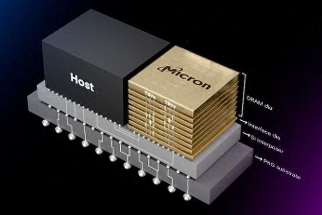
As for the N5 process, storage manufacturers can also choose to use TSMC N5 process to produce HBM4 basic chips. The basic chip constructed by the N5 process will encapsulate more logic, consume less power, and provide higher performance. The most important advantage is that this advanced process technology can reach a very small interconnection spacing, about 6-9 microns. This will make the N5 basic chip and the direct key combined, so that the HBM4 can perform 3D stacks on the top of the logical chip. Direct keys can achieve higher memory performance, which is expected to be a huge improvement for AI and high -performance computing (HPC) chips that always seek larger memory bandwidth.